Characterization of Microelectronic Devices
C. Fürböck, E. Gornik, M. Litzenberger, D. Pogany
Institut für Festkörperelektronik, Technische Universität Wien,
Floragasse 7, A-1040 Vienna, Austria
Temperature distribution in Smart Power ESD protection devices
(M. Litzenberger, C. Fürböck, D. Pogany, E.Gornik (in cooperation with Infineon Technologies, Munich, Germany)
The temperature distribution during and after an electrostatic discharge (ESD) has been investigated with ns time- and µm spatial resolution in ESD protection devices that are used in Smart Power integrated circuits for the automobile industry.
In this experiment the devices are stressed with ESD pulses of various current levels resulting in a heating of the device and a consequent change of the refractive index in the silicon (thermooptic effect). The change in the refractive index is measured with a heterodyne interferometric method via the phase shift in an infrared laser beam. The laser beam is directed from the chip backside on the device under investigation. It passes through the Si bulk and the active area of the device, is reflected on the front side metallization, passes back through the device and is focused on a detector, where it interferes with a reference beam that has a slightly different wavelength. From the resulting heterodyne signal the phase shift evolution in the probing laser beam during the ESD pulse is evaluated using a FFT algorithm. For the mapping of the temperature distribution, the active area of the device is automatically scanned with the laser beam, while the device is synchronously stressed with ESD pulses. The phase shift in the laser beam gives a measure for the integral of the refractive index change and therefore for the temperature increase along the laser beam path. To estimate the actual maximum temperature increase in the device, thermal simulations have been used to calculate the temperature distribution in the device along the laser beam path. From these data a correlation between the measured phase shift and the maximum temperature increase was derived.
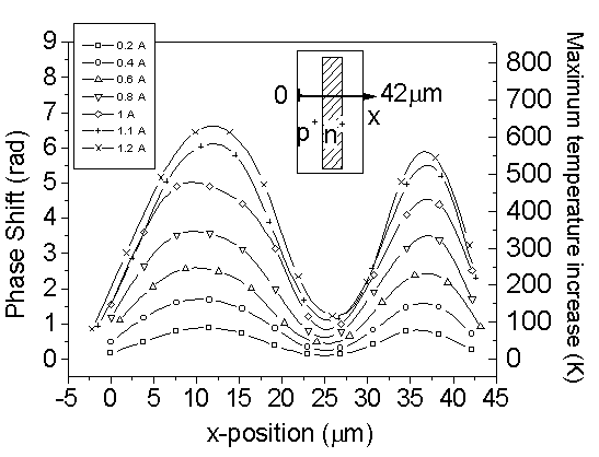
Figure 1 shows the cross section of the temperature distribution in a vertical npn transistor ESD protection device after stressing with currents from 0.2 A to 1.2 A. It can clearly be seen that the device is active (temperature increase) in the p+ regions of the structure, and inactive (no temperature increase) in the n+ (emitter) region (see inset), indicating that the bipolar transistor is not turned on and the device is operating before snapback. Also a slightly asymmetric shape of the temperature increase with higher values on the cathode side (left in the figure) can be identified. This asymmetry is due to the distributed resistance of the buried layer, resulting in a higher electric field and consequently in a higher current density at the cathode edge side of the device. Figure 2 shows the relation between the maximum temperature increase and the power of the ESD pulse, measured in four different types of ESD protection structures. It can be seen that the maximum temperature increase scales linearly with the pulse power. This is expected as the heat dissipated in the devices is proportional to the power of the stressing pulse, for the short times during the pulses. The results of measurements in many different types of ESD protective structures – in bipolar and also in CMOS technology – show that the method can identify critical parts in the layout and the functionality of the devices, even before they fail. This information is of great value for the device optimization, and this has already led to the improvement of the ESD ruggedness of the protection structures.
Fig. 1: The distribution of the phase shift and temperature in an ESD protection structure after stressing with an ESD pulse, shown for pulse currents from 0.2 A to 1.2 A. The layout of the structure (top view) and the location of the cross section are shown in the inset.
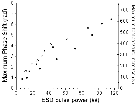
Fig. 2: The maximum phase shift and the maximum temperature increase depending on the ESD pulse power for 4 different device types (different symbols). As expected, the maximum temperature scales linearly with the power dissipation in the ESD protection device.
Laser interferometric method for ns-time scale thermal mapping of Smart Power ESD protection devices during ESD stress
(C. Fürböck, M. Litzenberger, D. Pogany, and E. Gornik)
Monitoring of breakdown homogeneity, temperature distribution, and thermal dynamics is of prime interest for the design and development of ESD protection structures. Selfheating effects during an ESD event are known to limit the performance and reliability of ESD protection devices. At our institute we use a laser interferometric thermal mapping technique to monitor the homogeneity of bipolar transistor action and temperature dynamics during ESD stress in ESD protection devices which are operated in the snap-back regime. The measured temperature profiles are compared to a thermal simulation and correlated with the positions of ESD damage obtained by backside IR microscopy. Critical places in the devices are identified under stressing conditions where no irreversible damage occurs which is important from the point of view of reliability evaluation and failure analysis.
The devices presented here are vertical pn diodes and laterally asymmetric npn transistor structures (see inset in Fig. 3). The temperature evaluation is based on monitoring the temperature-induced increase in the refractive index (thermo-optical effect) by measuring the phase changes of a non-absorbed infrared laser beam l = 1.3 µm) probing the device active region. The extracted phase shift (Fig. 3) is proportional to the integral of the temperature change along the probe beam path. The devices are stressed with 150 ns long current pulses. To estimate the temperature in the device we have simulated the vertical temperature profile in the device.
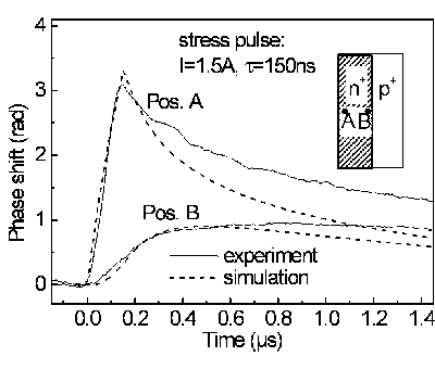
Fig. 3: Measured and simulated phase shift evolution for two positions in the asymmetric structure stressed by 1.5 A pulse of 150 ns duration. The delay in the signal maximum for the position B arises from the heat transfer from the dominant heat source (position A). The simplified layout of the structure is given in the inset.
At the position of the heat source, the phase shift exhibits a steep increase during the pulse and a decrease of the signal after current turn-off due to cooling of the device (Fig. 3, Pos. A). At positions outside the heat source the phase signal shows a delayed and reduced increase, which is caused by heat transfer from the dominant heat source (Pos. B). The simulated phase signal shows quantitative and qualitative agreement with the experiments during and after the ESD pulse, respectively (Fig. 3). At lower stress currents the temperature rise is homogeneous along the device width, whereas at higher current stress two hot spots are developed at the corners of the emitter area. (Fig. 4). These temperature peaks are well correlated with the position of the ESD damage found from infrared microscopy observation (Fig. 5).
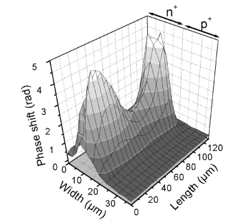
Fig. 4: Spatial distribution of the measured phase shift in an asymmetric structure at the end of a pulse with I = 1.5 A.
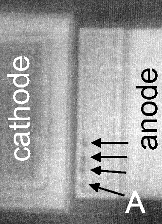
Fig. 5: IR image of the asymmetric structure which has been subjected to 4 ESD pulses of 1.9 A. The dark spots are indicated by arrows. The position of the first dark spot is denoted by ‘A’.
Our interferometric thermal mapping technique has shown a strong capability for investigating breakdown homogeneity, temperature distribution, and thermal dynamics in Smart Power ESD protection devices on a ns time scale with high spatial resolution. The increased temperature at the edge and corners of the n+ region of the asymmetric structure explains the position of the ESD damage in this device type. The IR camera observation of the ESD damages has revealed that the critical regions are the edges in asymmetric structure.
This work was performed in collaboration with Infineon Technologies in Villach (Austria) and Munich (Germany).
Stress evolution of low frequency (RTS) noise and leakage current in gg-nMOSFET ESD protection devices.
(D. Pogany, M. Litzenberger, C. Fürböck, E. Gornik (in collaboration with INFINEON and Siemens))
Electrostatic discharge (ESD) protection is an important issue for CMOS circuits. From the point of view of design optimization it is important to distinguish between surface and bulk failure modes in these devices. The surface degradation mode, especially the role of hot carriers during the ESD stress, is less studied. On the other hand, analysis of low frequency noise, especially random telegraph signals (RTSs), provides a sensitive tool to study surface related stress-induced damage in Si/SiO2 systems.
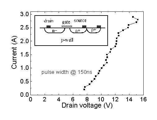
Fig. 6: Typical high current IV curve of an ESD protection device. Inset is the schematics of the structure; contact pads are indicated by black squares.
We have analyzed ESD stress-induced RTS fluctuations and leakage currents in 0.35 µm technology single finger grounded-gate (gg) n-channel MOSFETs with different layout parameters (see Fig. 6). Reverse IV curves and noise are monitored in the 0 – 3 V range after each gradually increased ESD stress pulse magnitude or number.
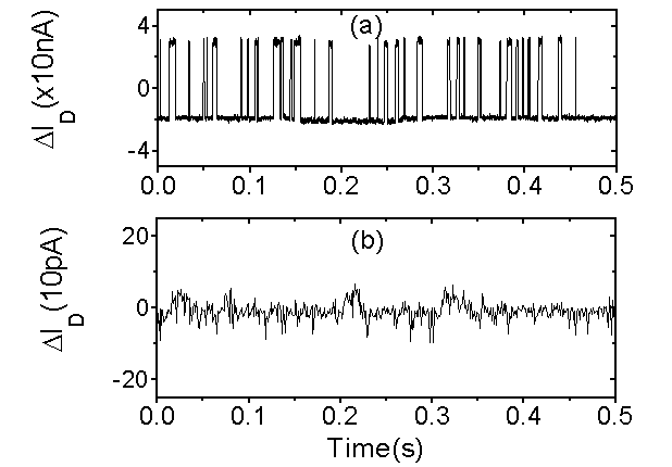
Fig. 7: Current fluctuations related to the strong non-monotone IV evolution (a) and gradual monotone IV behavior (b) in a gg-nMOS device stressed by 1.1 A and 1.6 A ESD pulse, respectively; VD = 2.2 V for both cases.
The results show two different stress evolutions of leakage current and noise which are typical by (i) strong increase in the current and noise and non-monotone evolution of IV characteristics which was attributed to surface (Si/SiO2 interface) origin of the ESD damage and by (ii) gradual monotone increase in IV characteristics and low noise which was attributed to a bulk ESD damage. The analysis of the ESD damage by the OBIC (Optical Beam Induced Current) technique supports the results of the electrical measurements.
Study of Random Telegraph Signal (RTS) noise in Smart Power DMOS devices
(D. Pogany and E. Gornik (in collaboration with INFINEON Technologies, Munich))
Double-diffused metal-oxide-semiconductor (DMOS) field effect transistors fabricated by smart power technology are widely used in the automotive industry as power switches. Structural or technology defects in power devices can cause a decrease in the breakdown voltage or an increase in the leakage current. It is important to identify possible sources of these defects in the early stage of technology development as they can have an impact on device reliability and lifetime. It has been shown in many studies that the leakage currents are often accompanied with the existence of excess low frequency noise. The 1/f or Random Telegraph Signal (RTS) noises are known as very sensitive indicators of device reliability and material quality.
We have studied low frequency current fluctuations in power multi-cell power DMOS devices in order to obtain information on the leakage current-related defects. We have established that an excess leakage current is always accompanied by an excess low frequency noise which has a form of RTS fluctuations or 1/f noise. The relative RTS amplitude DID/ID as a function of ID exhibits first a plateau followed by a roll-off having an ID-a dependence with 0.5 < a < 1. The typical relative RTS amplitude values at the plateau are close to 1%, but RTS fluctuations with the relative amplitude as high as 20% have also been found (see Fig. 8). The RTS noise in the frequency domain (0.1 Hz – 10 kHz range) gives rise to a Lorentzian spectrum superimposed on a 1/f noise background which indicates that the dominant RTS noise is governed by a Poisson process (Fig. 9). As going to higher gate biases (VG > 1.6 V, inversion), the noise is dominated by a 1/f spectrum in any device.
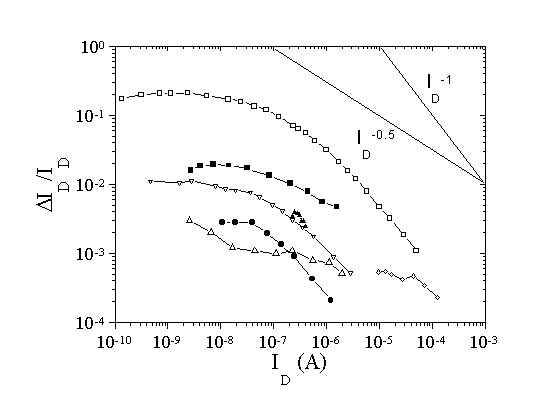
Fig. 8: Relative RTS amplitude DID/ID as a function of ID for seven different devices with and without the excess leakage current at VG = 0. Two different slopes in the DID/ID–ID dependence are indicated by solid lines.
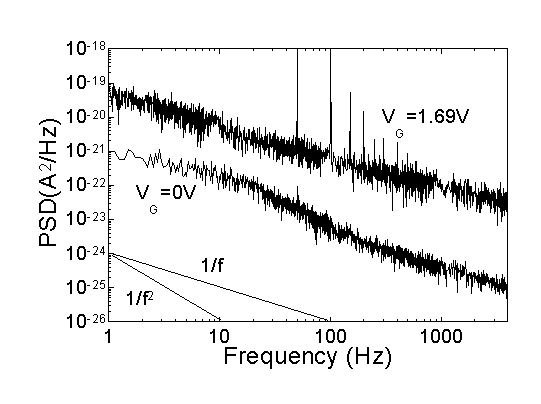
Fig. 9: Frequency dependence of power spectral density (PSD) at two different gate biases of a DMOS exhibiting RTS noise. Note the curve at VG=1.69V is typical also for defect-free devices.
The results indicate that the basic noise mechanism in these multicell devices is similar to the noise mechanism observed in submicron MOSFETs (carrier trapping/detrapping at or near Si/SiO2 interface under the gate oxide). For simplicity, the DMOS structure is considered as a parallel connection of submicron MOSFETs. Each of these MOSFETs exhibits RTS (or 1/f) fluctuations which, in superposition, give rise to 1/f noise in the inversion. The observation of the single RTS fluctuators in the devices with the excess current indicates that the leakage current and noise comes from one single or a small number of cells. The leakage current is supposed to be due to an extended defect located in the device active area. The structural analysis has revealed crystal damage in the body/drain and body/source region, which confirms the conclusion driven from the noise study.
Damage analysis in Smart Power technology ESD protection devices
(D. Pogany, M. Litzenberger, E. Gornik (in collaboration with INFINEON and Siemens))
Electrostatic discharge (ESD) protection devices are of great importance in smart-power technology circuits used in the automotive industry. Temperature rise during the ESD stress may induce fatal device failure due to thermal instability during the second breakdown. Analysis of the ESD damage is therefore an important issue for the design optimization of these devices. We have studied damage caused by ESD stress in Smart Power technology ESD protection devices using backside IR microscopy and IV characterization.
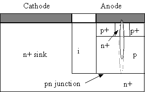
Fig. 10: Schematics cross section of a symmetric ESD protection device. The model of the damaged region is also shown: solid and dotted ellipses indicate defects outside and inside the zero bias space charge region.
Devices used in this study are vertical pn diodes and laterally symmetric and asymmetric npn transistor structures with a breakdown voltage near 60 V (see Fig. 10). The ESD damage, seen in the infrared camera as a dark spot (DS), is caused by the local thermal degradation of the Si/(contact metallization) interface due to current filamentation. In general, the successive stress causes either (i) a creation of a new DS usually accompanied with a kink in IV characteristics (new leakage path) or (ii) an increase in dimension of an already existing DS connected with a shift of the kink to lower voltages. We have also established that the increase in the reverse leakage current at low biases is always accompanied with the increase in the forward leakage current at low forward biases (Fig. 11). If the reverse current increase is observed at higher voltages, the forward current is unaffected.
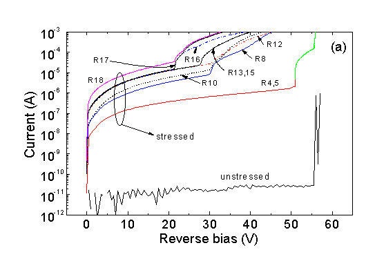
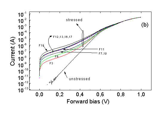
Fig. 11: Development of reverse (a) and forward bias (b) IV curves as a function of increasing stress pulse number (3 A) in an asymmetric structure exhibiting two DSs in the n+ emitter region. The same number in the numbering of the curves in (a) and (b) corresponds to the same stress level. The reverse leakage current components at VR < 20 V and VR > 20 V (kinks) correspond to stress evolution of either DSs. Note that the increase in the reverse current at low voltages, but not the kink component, is correlated with the increase in the forward bias leakage.
From the experiments we assume that the DS region is formed by a high density of g-r centers, probably due to diffusion of impurities from the contact metal. The progressive decrease in the kink voltage observed in the reverse IV curves is interpreted as a stress-induced penetration of the defect region through the reverse bias space charge region. The penetration of the damage into the zero-bias space charge region causes an increase in the forward current where the defects act as recombination centers. From the simulation we have estimated that the forward current increase starts to be observable when the damage penetrates 4.7 µm from the surface.