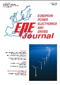
EPE Journal, "European Power Electronics and Drives", Volume 17, N° 2, 2007.
Copyright - [Précédente] [Première page] [Suivante] - Home
Fiche : [REVUE678]
Titre : EPE Journal, European Power Electronics and Drives, Volume 17, N° 2, 2007.
Cité dans : [DIV322] Les revues EPE Journal et EPE Newsletter, février 2011.
Volume : 17
Numero : 2
Date : 2007
Site_web : http://www.epe-association.org/epe/main.htm
Stockage : Thierry LEQUEU
Vers : Active Compensation for Supply Voltage Unbalance on Two-stage Direct Power Converter
Vers : Improvement Schemes of Control Performance for Matrix Converter
Vers : Design and Comparison of Two Multilevel Converters for Flicker Compensation
Vers : Linerization of multi-level SVPWM signal generation in over-modulation region extending to 6-step mode using the sampled amplitudes of reference phase voltage
Vers : Associative methods for d.c./d.c. power electronics control
Vers : Small-Signal Modeling and Analysis of DC Distributed Power Systems

EPE Journal Volume 17-2 - Editorial
EPE 2007, Aalborg, Denmark, goes strongly renewable [Details]
By Frede Blaabjerg
The editorial of EPE Journal Volume 17-2: EPE 2007, Aalborg, Denmark, goes strongly renewable, written by Prof. Frede Blaabjerg, Conference Chair of EPE 2007
By T. Wijekoon; C. Klumpner; P. Wheeler
It is known that the output voltage capability of Matrix Converters (MC), which has no energy storage, is seriously affected when the supply voltage is unbalanced. Passive compensation methods improve the waveform quality of the output, but provide reduced output voltage depending on the level of unbalance. This paper proposes an active compensation technique for unbalanced supply voltages in the two-stage Direct Power Converter (DPC). The technique is based on the utilisation of the clamp capacitor, which is normally needed to protect a MC, to extend the operating range of a two-stage DPC during unbalanced supply, preserving its theoretical output voltage capability. A comprehensive simulation study with analytical explanations justifies the proposed method. Experimental results using a laboratory prototype confirms the viability of the proposed active compensation technique.
By H. Ohguchi; J-I. Itoh; I. Sato; A. Odaka; H. Kodachi; N. Eguchi
This paper proposes improvement schemes of the voltage control performance for the matrix converter. The voltage control performance is deteriorated because of the commutation method, the output voltage error, and the input voltage disturbance such as the input voltage distortion and unbalance, in general. Firstly, two types of the commutation methods are described in this paper. The switching loss is compared through simulations, and the converter efficiency is compared through experiments on the two methods. Secondly, the output voltage error is analyzed and an error compensation scheme is proposed in this paper. The experimental results show the THD of the output current can be decreased with the proposed compensation. Finally, in order to decrease the distortion of the output voltage in case of the input voltage disturbance, a novel compensation method for the input voltage disturbance is proposed. The adequacy of the method is proved by simulations and experiments. Motor drive characteristics of a 22kW proto type matrix converter, equipped with the proposed methods, are also shown.
By G. Buja; S. Castellan
The paper is concerned with the design of multilevel converters for compensating the flicker on the medium-voltage distribution networks. Two topologies of converters are considered, namely the Diode Clamped MultiLevel Converter (DCMLC) and the Cascade H-bridge MultiLevel Converter (CMLC). By analytical procedure, the current ratings for the semiconductor devices of the converters are determined, and their passive elements are sized up. The main outcome of the study is that the two topologies substantially require the same overall rating for the semiconductor devices, with the exception of the clamping diodes in the DCMLC-based topology. As a counterpart, the latter topology needs a lower overall capacitance.
By R. S Kanchan; P. N Tekwani; K. Gopakumar
The correct full title is: Linearization of the multi-level SVPWM signal generation in the over-modulation region extending up to six-step mode using only the sampled amplitudes of reference phase voltages
A multi-level PWM signal generation with linear transfer characteristics between fundamental component of output voltage and modulation index is proposed in this paper for a n-level SVPWM signal generation. The reference signal to the PWM modulator is pre-scaled in over-modulation region, keeping the fundamental component of the modified signals same as the original signal. The modified reference signal is always confined within the carrier region. Thus linear transfer characteristics can be extended throughout the over-modulation region up to six-step mode to get the maximum utilization of DC link, for multi-level inverter drive control of any general n-level. In this paper, the principle of pre-scaling the reference signal, based on a look up table, for two-level PWM generation is extended to a general n-level SVPWM. The whole PWM signal generation is implemented using only the sampled amplitudes of reference phase voltages and the algorithm is very suitable for real time implementation on DSP processors. A five-level inverter configuration, using an open-end winding induction motor drive, is used for verifying the SVPWM generation scheme, experimentally.
By D. Alejo; P. Maussion; J. L. Faucher
This paper describes two different control principles using simple combinations between basic control laws. The objective is to improve the performance (time response, overshoot, robustness
), without strongly increasing the complexity. These principles are tested on a d.c.-d.c. power converter. Linear and/or non linear controllers are mixed depending on the optimisation objective and on the decision data. The basic idea is that in the world of control, as elsewhere, unity is strength, i.e. complex functions could be carried out through basic object combinations. The first principle is based on the combination of two linear controllers. Only two models of the system are taken into account in this Multi Model Control (MMC) method. A new and specific procedure for model validity is put forward. It is based on the distance between two extreme models of the controlled system, with unknown severe disturbances. The second principle suggests the combination of a linear controller and a non-linear controller (a Bang Bang and an Integral and Proportional controller). This combination is created through the fuzzy fusion of state variables. The tuning of the fuzzy logic parameters is made through Hooke and Jeaves optimisation procedure. The performance is verified through experimental results on a d.c./d.c. converter application. They are significantly improved with respect to standard controllers, with only one voltage sensor and without any adaptive gains.
By P. Karlsson
DC power systems have been discussed for connection of renewable, small-scale power generation units. The investigated DC power system is based on a ring bus structure with voltage source converters connected back-to-back (Fig. 1). This paper addresses small-signal analysis of DC distributed power systems with emphasis on converter modeling and DC bus voltage control. Droop control (Fig. 2) is utilized to distribute the load between the source converters. The dynamic properties in terms of small-signal stability are investigated both for the converters and for small DC distribution systems. First a two-converter system and then a three-converter system are investigated. Stability is investigated in terms of frequency responses and pole-zero maps. It is found that the converter models do not have to be taken into account. It is also found that the negative equivalent small-signal resistance of constant power loads does not cause instability, for the proposed converter and investigated DC bus parameters. Load sharing is also investigated with frequency responses. Simulation results based on the analyzed small-signal model is compared to both large-signal simulations and experimental results.
Mise à jour le lundi 26 janvier 2026 à 18 h 42 - E-mail : thierry.lequeu@gmail.com
Cette page a été produite par le programme TXT2HTM.EXE, version 10.7.3 du 27 décembre 2018.
Les informations contenues dans cette page sont à usage strict de Thierry LEQUEU et ne doivent pas être utilisées ou copiées par un tiers.
Powered by www.google.fr, www.e-kart.fr, l'atelier d'Aurélie - Coiffure mixte et barbier, Maelline Travel Planner - Organisatrices de voyage sur mesure, La Boutique Kit Elec Shop and www.lequeu.fr.


